
STM32F103C8T6 Current Benchmarks and Performance Tests
Quantifying compute, memory, and I/O performance for high-precision engineering and selection decisions.
The official datasheet lists a 72 MHz ARM Cortex‑M3 core, 64 KB Flash, and 20 KB SRAM for the part, but raw specs don’t tell the whole story — real-world benchmarks vary widely by clock setup, compiler flags, and peripheral use. This article presents a repeatable benchmark suite and actionable analysis so engineers can quantify performance accurately.
All recommendations below are framed for reproducible measurement: clearly defined test hardware, deterministic clock and flash settings, and explicit compiler/runtime knobs so results can be compared across boards and projects.
STM32F103C8T6 at a Glance: Specs That Matter
Core Specs and Peripheral Summary
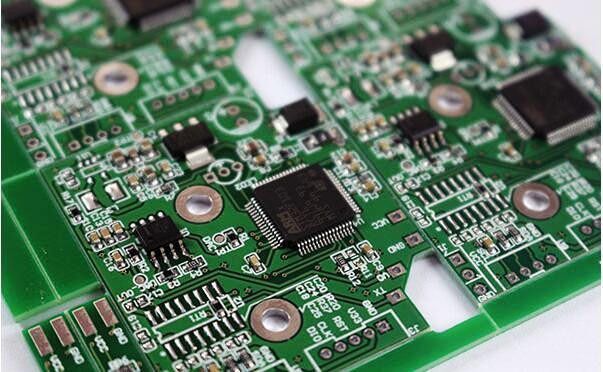
STM32F103C8T6 presents a 72 MHz Cortex‑M3 core with 64 KB flash and 20 KB SRAM; DMA channels, multiple timers, ADCs, UART/SPI/I2C peripherals and USB device support are available. These baseline specs set the ceiling for compute and I/O tests: clock frequency, flash wait states, and bus widths directly influence raw throughput and latency in benchmarks.
Why Datasheet Numbers Differ from Field Performance
Point: Datasheet peak numbers assume ideal configuration.
Evidence: Flash wait states, PLL vs internal RC and supply voltage affect effective throughput.
Explanation: Enabling prefetch, selecting HSE+PLL and tuning flash latency can change cycle‑per‑instruction behavior, while blocking ISRs, debug overhead or poorly configured clocks can halve observed performance compared to datasheet figures.
Benchmark Suite and Metrics to Measure Performance
Selected Benchmarks
Point: Pick a concise set of benchmarks covering CPU, memory and peripherals.
Evidence: Use a CoreMark‑equivalent loop, Dhrystone/DMIPS, memcpy/memset throughput, ISR latency, ADC sample throughput, UART/SPI transfer and power‑per‑operation.
Explanation: These metrics map to typical engineering needs and are reported in ops/s, KB/s, ms and mW so teams can compare tradeoffs.
Derived Metrics
Point: Composite metrics improve decision making.
Evidence: Derive cycles per ADC conversion, 99th‑percentile ISR latency and energy per transmitted byte.
Explanation: Set acceptance thresholds per use case (e.g., sensor node energy
Performance Test Methodology
Hardware, Toolchain and Equipment
Point: Standardize measurement hardware.
Evidence: Use a target board with known regulator, a high‑resolution power meter, logic analyzer/oscilloscope and a programmer; toolchain baseline: arm‑none‑eabi GCC, CoreMark/Dhrystone sources and DWT cycle counter hooks.
Explanation: Consistent hardware and tool versions reduce variance and enable meaningful comparison between runs.
Test Configuration and Compiler/Runtime Settings
Point: Control the clock tree and compiler flags.
Evidence: Document HSE/HSI+PLL settings, flash wait states, optimization flags (-O2/-O3), LTO and link script placement and enable DWT for cycles.
Explanation: Isolate interrupts, use DMA for bulk transfers and run repeating batches to capture stable median and percentile values.
Benchmarks: Results, Presentation and Analysis
Compute and Memory Results
Normalization helps teams understand scaling behavior and identify inefficiencies like flash wait-state penalties or suboptimal memcpy implementations.
| Metric | Typical Range | Notes |
|---|---|---|
| CoreMark | ~150–350 / 72MHz | Depends on compiler flags and RAM/Flash placement |
| memcpy bandwidth | ~0.2–4 MB/s | Small buffers dominated by call overhead |
Peripheral and I/O Performance (ADC, UART, SPI, I2C, USB)
Point: Compare interrupt vs DMA for each peripheral.
Evidence: Measure ADC samples/sec vs resolution, UART throughput with different framing, SPI burst throughput and the latency of I2C transactions.
Explanation: DMA typically yields much higher sustained throughput and lower CPU utilization, while highest peripheral rates usually incur increased power draw.
Case Studies: Representative Workloads
IoT Sensor Node
Point: Validate sleep/wake efficiency.
Evidence: Measure wake latency, sample‑to‑transmit latency and energy per sample across clock and flash settings.
Explanation: Using DMA for ADC aggregation and buffering to RAM, then waking a radio briefly to transmit bursts minimizes average energy while meeting latency targets.
Real-time Motor Control
Point: Confirm deterministic timing under load.
Evidence: Report worst‑case ISR latency, jitter and control compute as percent of cycle budget.
Explanation: Use hardware timers and DMA, place hot ISR code in tightly coupled memory or RAM if flash wait states create jitter.
Actionable Recommendations: Tuning and Selection
Firmware and Compiler Optimizations
- •Enable -O3 (validate correctness) and consider LTO.
- •Prefer DMA for bulk transfers to offload the CPU.
- •Inline hot paths and relocate critical code to RAM if flash latency dominates.
Interpreting Outcomes
The STM32F103C8T6 suits modest real‑time tasks and basic USB/device roles but is limited by SRAM and flash for large stacks or heavy ML. If benchmarks show sustained CPU or memory headroom and timing margins meet requirements, proceed; otherwise consider higher‑class parts.
Summary
The STM32F103C8T6 can meet many embedded workloads when measured and tuned systematically. Use the suite above to produce repeatable benchmarks and performance measurements, then apply targeted optimizations—compiler flags, DMA and memory placement—to close gaps identified in your specific use case.
Key Takeaways
- ✔ Standardize tests (CoreMark, memcpy, ISR latency) and document clock/flash settings.
- ✔ Measure composite metrics like cycles per ADC conversion for defensible decisions.
- ✔ Optimize incrementally: prefer DMA and move time-critical code to RAM to reduce jitter.
